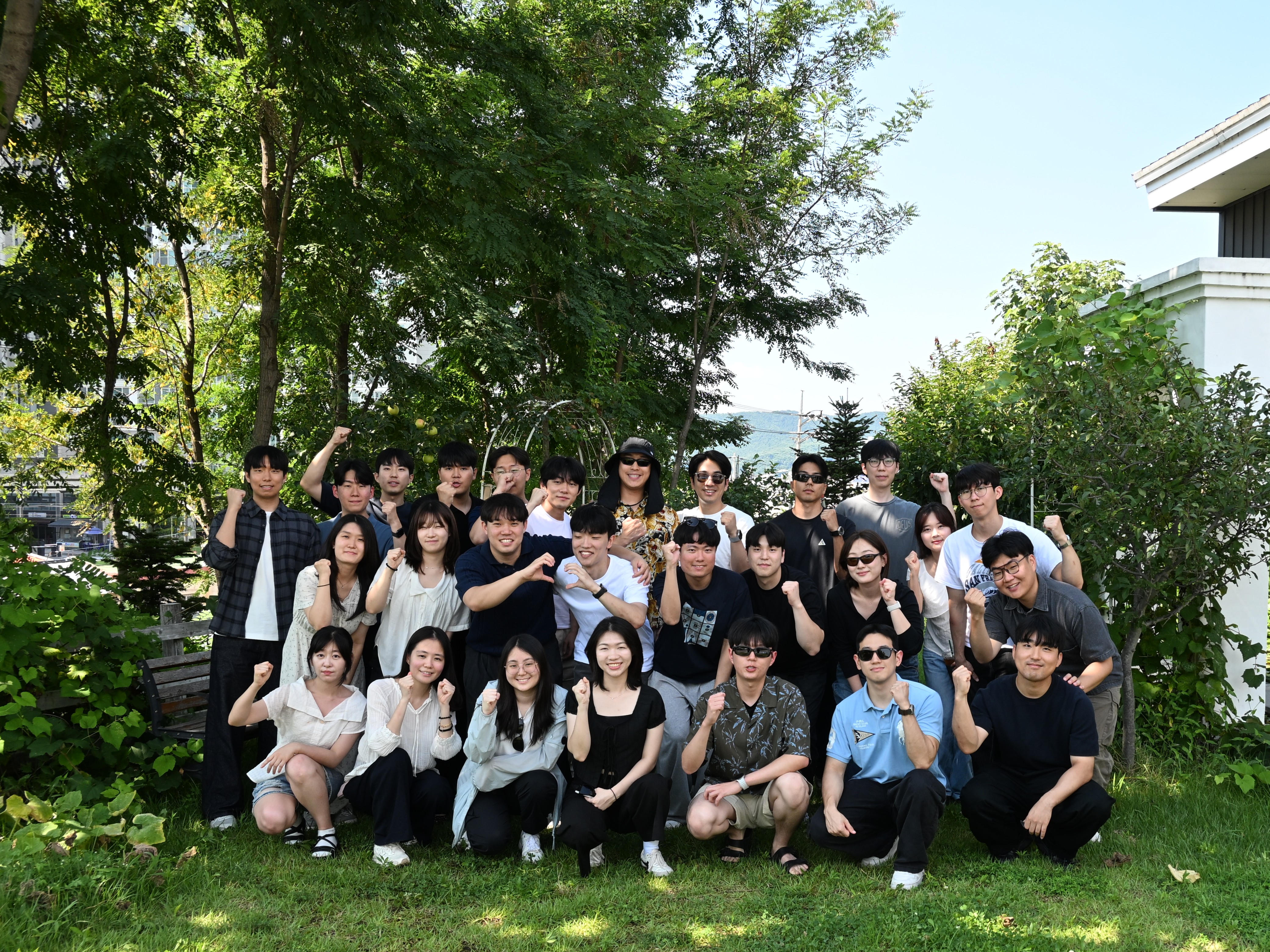
26-spring_outing
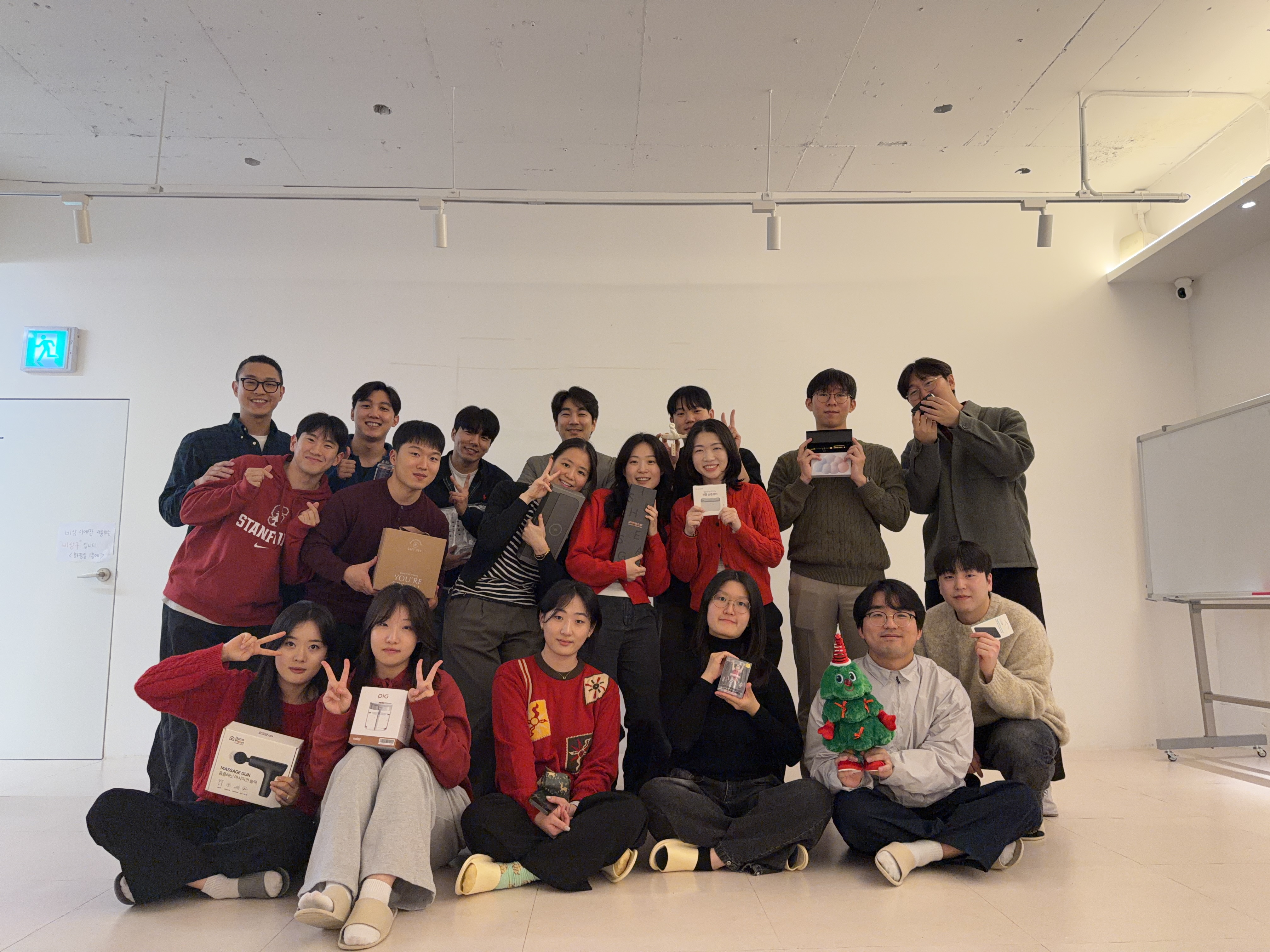
25-winter_year-end-party
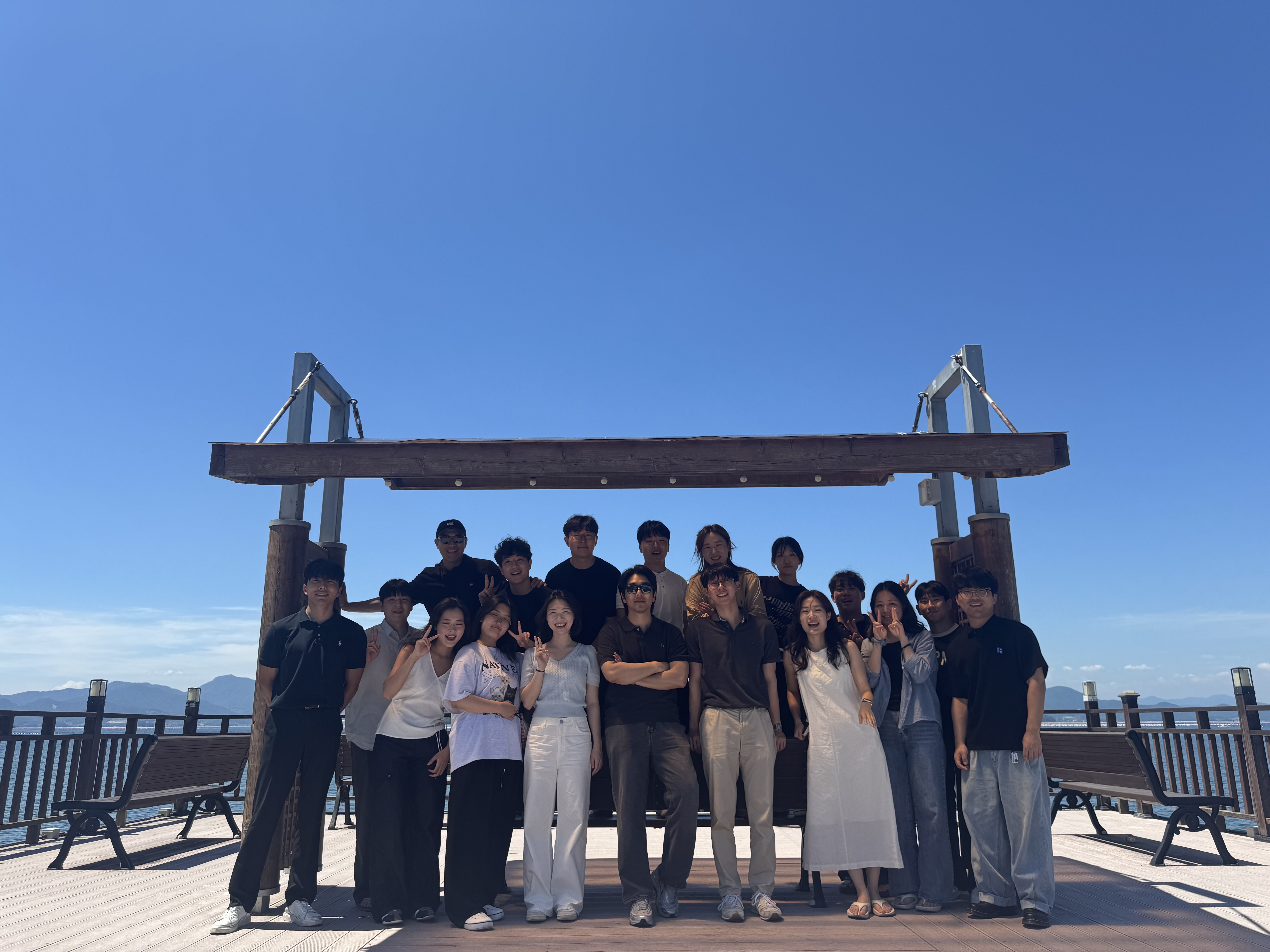
25-summer_mt
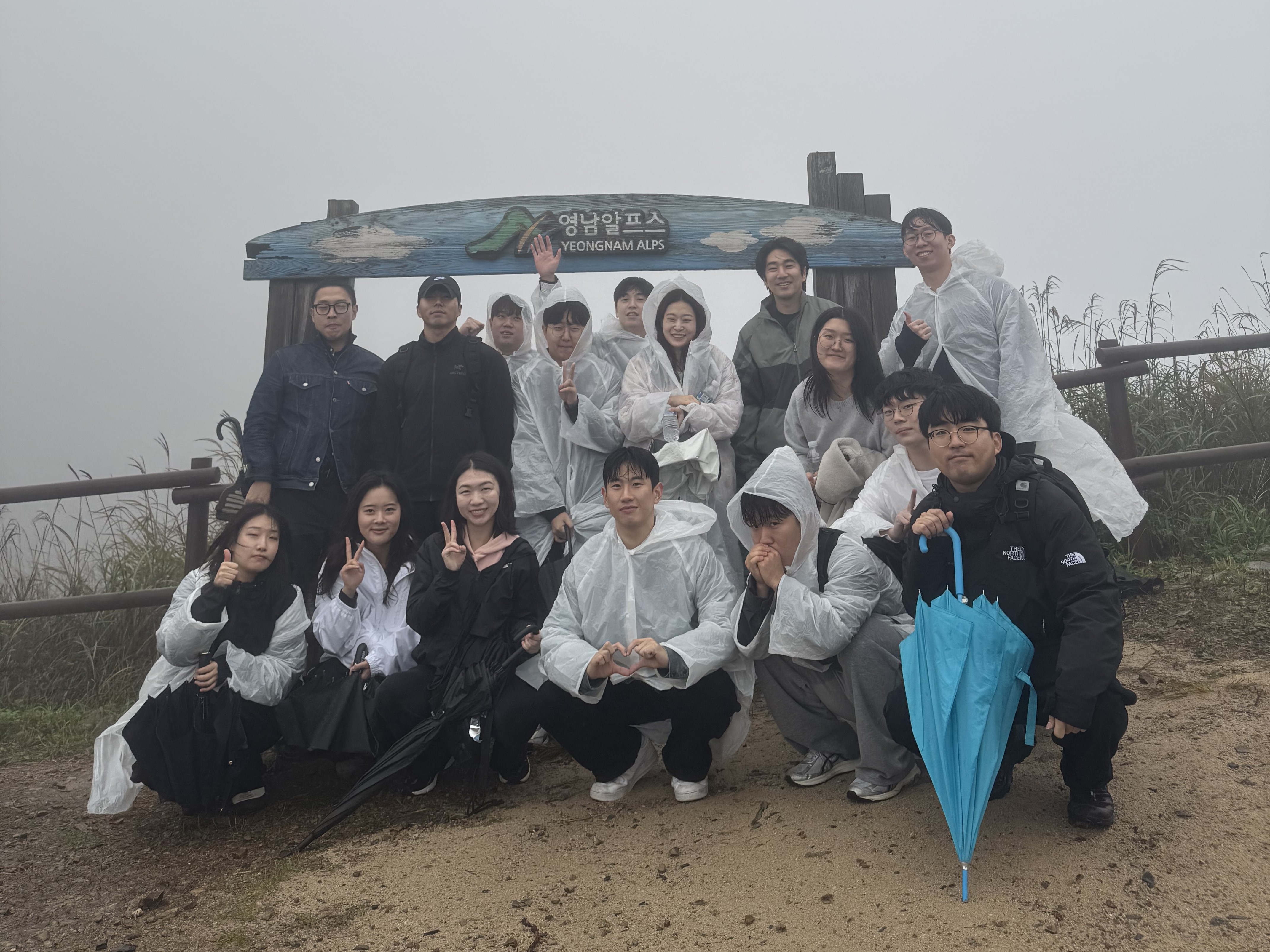
25-fall_ganwolche

KAIST Device-to-System Integration Lab (DSIL)

우리 연구실은 차세대 AI 하드웨어 시스템을 위한 핵심 반도체 기술 개발을 목표로 합니다. 이를 위해 전기전자공학을 중심으로 기계공학, 재료공학, 화학공학을 융합한 다학제적 접근을 통해 소자–패키징–시스템을 연결하는 통합 반도체 기술을 연구하고 있습니다.

Contact

현재는 오랜 호흡으로 박사까지 진학할 학생이나 통합 과정 지원자를 우선적으로 선발합니다. 관심 있는 분들은 CV, 성적표, 연구 활동 자료 (논문, 프로젝트 등)를 제 메일로 보내주시기 바랍니다 (jmkwon@kaist.ac.kr).

최신 뉴스

전체 보기
  • 이용우 박사후연구원이 교육부와 한국연구재단이 지원하는 ‘Post-Doc. 성장형 연구지원’ 사업의 단독연구 유형에 선정되었습니다.

  • 과제명 : Physical AI 휴머노이드를 위한 고신뢰 유리기판 기반 mmWave GaN RF PA 내장 패키징 원천기술 연구 (link)

본 사업은 유망한 박사후연구원이 전임교원의 멘토링 아래 혁신적이고 도전적인 연구를 수행하며 독립연구자로 성장할 수 있도록 3년동안 연간 0.6억원을 지원합니다.

  • 제목: Oxygen-Tunnel Indium Tin Oxide Vertical Channel Transistors with Enhanced Current Density and Reliability for Monolithic 3D Compute-In-Memory Systems 본 연구에서는 인듐주석산화물(ITO) 수직 채널 트랜지스터에 산소 터널(SiN/SiO₂/SiN) 구조를 적용하여, 구동 전류와 소자 신뢰성을 동시에 향상시키는 기술을 제안하였습니다.이를 통해 모놀리식 3차원 집적(Monolithic 3D) 기반 임베디드 메모리 구현 가능성을 제시하였습니다.

제안한 구조는 산소의 이동을 정밀하게 제어하여 전극의 산화를 억제하는 동시에 ITO 채널을 안정화함으로써, 최고 수준의 전류밀도인 436 μA/μm와 우수한 바이어스 스트레스 안정성을 달성하였습니다. 또한, 이러한 소자를 기반으로 축전기(capacitor)가 필요 없는 게인셀 메모리를 구현하여 648초 이상의 데이터 유지 특성(retention)과 1,200회 이상의 쓰기/읽기(write/read) 동작을 성공적으로 입증하였습니다.

시스템 수준의 평가에서는 Si-CMOS와 ITO 소자의 하이브리드 집적을 통해 메모리 셀 면적을 줄이는 동시에 데이터 유지 시간을 연장하고, 차세대 AI 하드웨어를 위한 컴퓨트-인-메모리(Compute-in-Memory) 성능을 향상시킬 수 있음을 보였습니다. 본 연구는 한국연구재단, 한국산업기술기획평가원 및 과학기술정보통신부, 산업통상자원부의 연구개발 지원을 받아 수행되었습니다.

Join Us

전체 보기

I/O Circuit Design for Multi-Chip Systems

Design and Benchmark (DB) or Component Packaging (CP)

This position focuses on the design of IO circuits — particularly logical PHY for die-to-die (D2D) interconnects — that form the backbone of future...

More

VCT based Oxide DRAM

Technology Development (TD), Memory

The Memory Team focuses on oxide-semiconductor-based 2T0C DRAM, pursuing an integrated research framework that spans device architecture, fabrication processes, materials, circuits, and system-level design...

More

Agent AI for Semiconductor System

개별연구 학생 (Undergraduate Internship)

This position focuses to establish a next-generation AI-native semiconductor design framework that enables integrated optimization across the Device–Circuit–Package–System stack. It includes AI-based standard cell...

More

High Performance Logic Devices

Technology Development (TD), Logic

This position focuses on advanced CMOS technology development by investigating low-dimensional (2D/1D) transistors through experiments and TCAD simulations. The research extends device concepts to...

More

Standard Cell Design and Benchmarking for 3D-Stacked FETs

Design and Benchmark (DB), DTCO

This position focuses on evaluating and abstracting the physical characteristics of silicon 3D-stacked FETs and novel-material devices from the standard-cell perspective. Building on this...

More

System-Level Benchmarking of Advanced Devices and Packaging Technologies

Design and Benchmark (DB), STCO

This position focuses on system-level benchmarking of advanced devices and packaging technologies. The candidate will work on evaluating the performance, energy efficiency, and scalability...

More

Advanced Packaging Technologies

Components and Packaging (CP), Packaging

This position focuses on integrated electrical, mechanical, and thermal design, experimentation, measurement, and development for high-speed signal transmission based on advanced packaging building-block technologies....

More