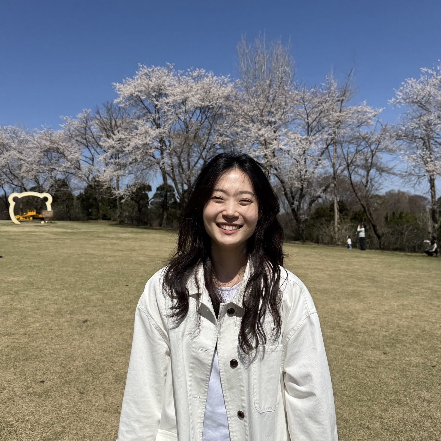
Yurim Choi
January 2024 – July 2026
- MS Student
- UNIST Nanoelectronics and Advanced Packaging Lab (UNL) MS Student, CP Team
- Packaging Metallization Process (Cu Pillar Bumps, RDL, and Build-up Layers)
- Electromagnetic Interference (EMI) Analysis for Packaging Interconnections
Current: Samsung SDI
BIO
Ms. Yurim Choi was a Master's student in the UNIST Nanoelectronics and Advanced Packaging Lab (UNL) and a core member of the CP Team from January 2024 to July 2026. As one of the lab's foundational members, she established the electroplating process from the ground up, successfully defining the metallization processes for packaging components such as Cu pillar bumps, RDLs, and build-up layers—which have now become integral to the lab's fabrication workflow. Leveraging this infrastructure, she advanced the lab’s capabilities by performing actual flip-chip assemblies for empirical measurements. These pioneering process achievements culminated in a publication at the IEEE Electronic Components and Technology Conference (ECTC), the premier global event in the field of semiconductor packaging. Her research also made significant strides in electromagnetic interference (EMI) analysis for packaging interconnections; by rigorously aligning experimental transmission line data with EM simulation results, she successfully integrated realistic physical parameters into the models, drastically improving simulation accuracy. This groundbreaking work bridging fabrication and simulation led to a top-tier academic milestone, being published as a co-first author at the IEEE International Electron Devices Meeting (IEDM), the world’s most prestigious conference in semiconductor devices. Beyond her remarkable technical achievements, Yurim was a driving force behind the lab's culture. She approached every research bottleneck with an enterprising spirit and a relentless passion for problem-solving. Universally known for her deep empathy and genuine warmth, she continuously infused the lab with vibrant energy and camaraderie. Her technical legacy and the bright, uplifting presence she brought to the team leave an enduring mark on UNL. She is currently pursuing her professional career at Samsung SDI.
Career
- Samsung SDI (July 2026 - present)
Education
- MS / Department of Electrical Engineering, UNIST (Jan 2024 - July 2026)
- BS / Department of Electrical and Information Engineering, Ajou University (Mar 2019 - Feb 2023)
Publications in Lab
Conference
-
3D printed fanout interposer substrates with curved through-holes for rapid prototyping of advanced packaging
-
Quasi-coaxial through-hole integrated additively manufactured antenna-in-package lid substrates
-
Monolithic 3D integration of III-V HEMTs on glass using ultra-thin dielectric bonding layer: a high-frequency and low-loss active glass platform for sub-THz applications
-
Active BSCDN benchmark framework with backside-compatible CNFET logic technology
-
Vertical-die (v-die) 3.5D integration for cool ultrahigh-bandwidth memory systems
-
Signal integrity challenges and opportunities in high-density chiplet I/O on glass substrates
-
Analysis of shrinkage-induced dimensional mismatch in 3D-printed packaging substrates for flip-chip bonding