◀ Back to list

Logic

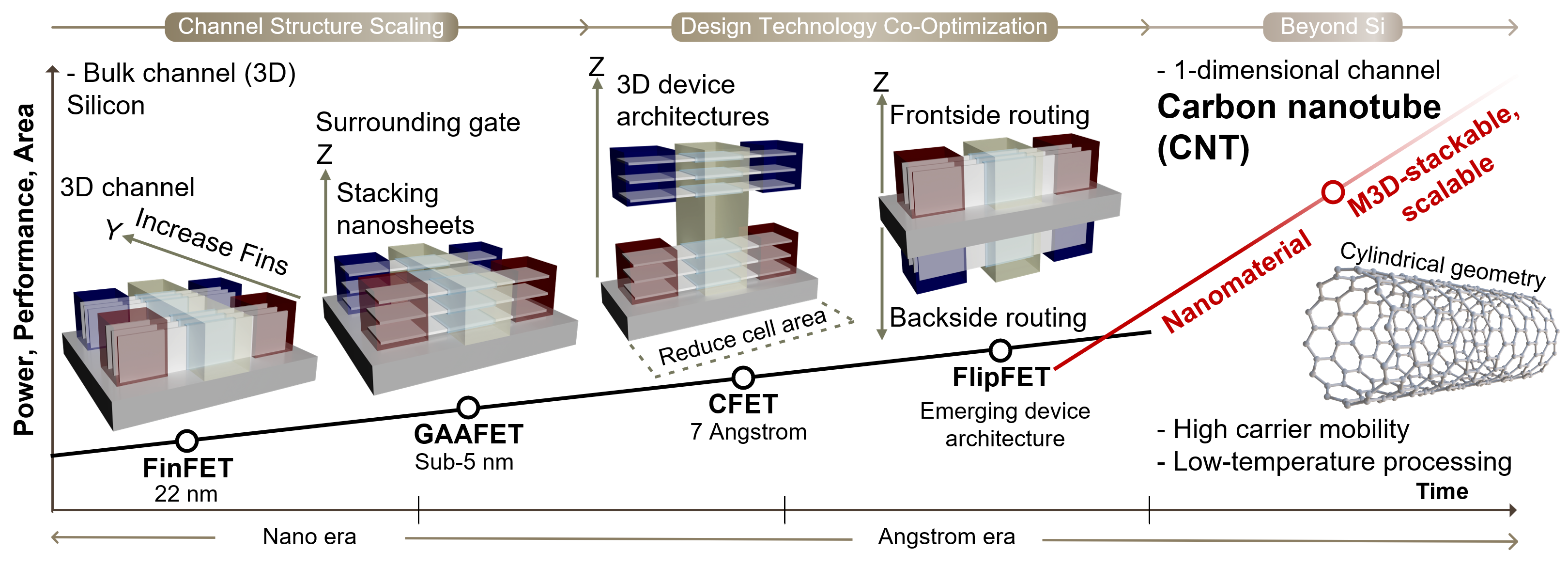
As silicon field-effect transistors approach their fundamental downscaling limits, maintaining performance gains through conventional scaling has become increasingly challenging. To address these limitations, advanced device architectures—such as gate-all-around (GAA) FETs, complementary FETs (CFETs), and FlipFETs—along with emerging low-dimensional channel materials, are being actively explored for next-generation logic. Low-dimensional materials, including two-dimensional transition metal dichalcogenides (TMDs) and one-dimensional carbon nanotubes (CNTs), are particularly attractive due to their excellent electrical properties at scaled dimensions and their compatibility with low-temperature, BEOL-compatible processes. These characteristics make them promising candidates for monolithic 3D integration. enabling sequential device stacking and vertical integration.

Two-dimensional transition metal dichalcogenides (TMDs)

Single-crystalline 2D channel

This work aims to establish a comprehensive framework for employing two-dimensional (2D) semiconductors as channel materials in transistor devices. We first investigate 2D single-flake transistors, focusing on how flake thickness and material uniformity influence electrical characteristics through systematic and statistical analyses. Building on the insights obtained from single-flake devices, we further extend our study to device fabrication using transferred 2D film-based transistor performance. Through this continuous research flow, we seek to bridge fundamental material understanding and practical device implementation of 2D semiconductor channels.

High performance TMD FETs

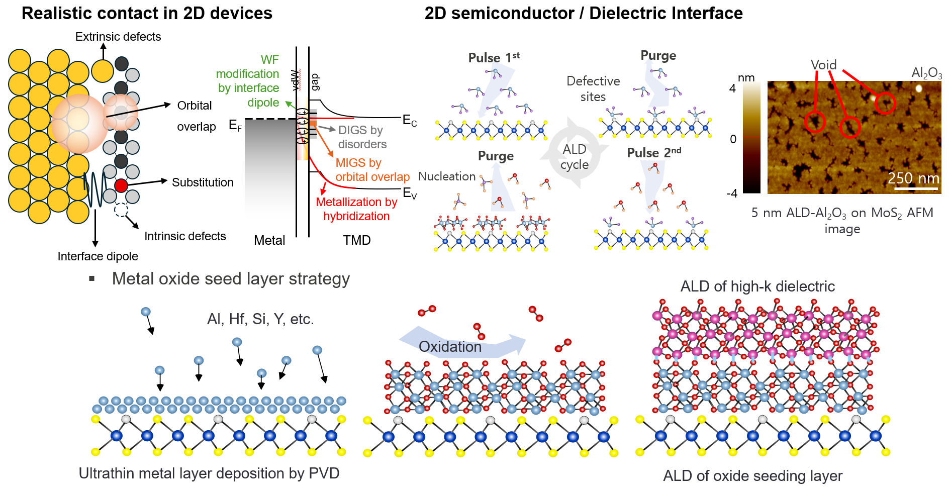
This research aims to enhance performance and reliability to enable the commercialization of two-dimensional (2D) semiconductors as transistor channel materials. Focusing on logic-compatible, top-gated 2D FETs, we address key challenges arising from the ultrathin of 2D materials, including high contact resistance and difficulties in forming a uniform, high-quality gate stack. To overcome these issues, we perform contact engineering and seed-layer/interfacial engineering to achieve conformal dielectric deposition, and we quantitatively investigate electrical characteristic variations and reliability metrics at the single-flake level. Building on insights from single-flake devices, we further expand the scope to wafer-scale, large-area device fabrication by adopting 2D film processing, thereby validating the feasibility of 2D channels in realistic integration environments and advancing toward nanoscale device fabrication and scaling.

One-dimensional carbon nanotubes (CNTs)

High density aligned CNT channel

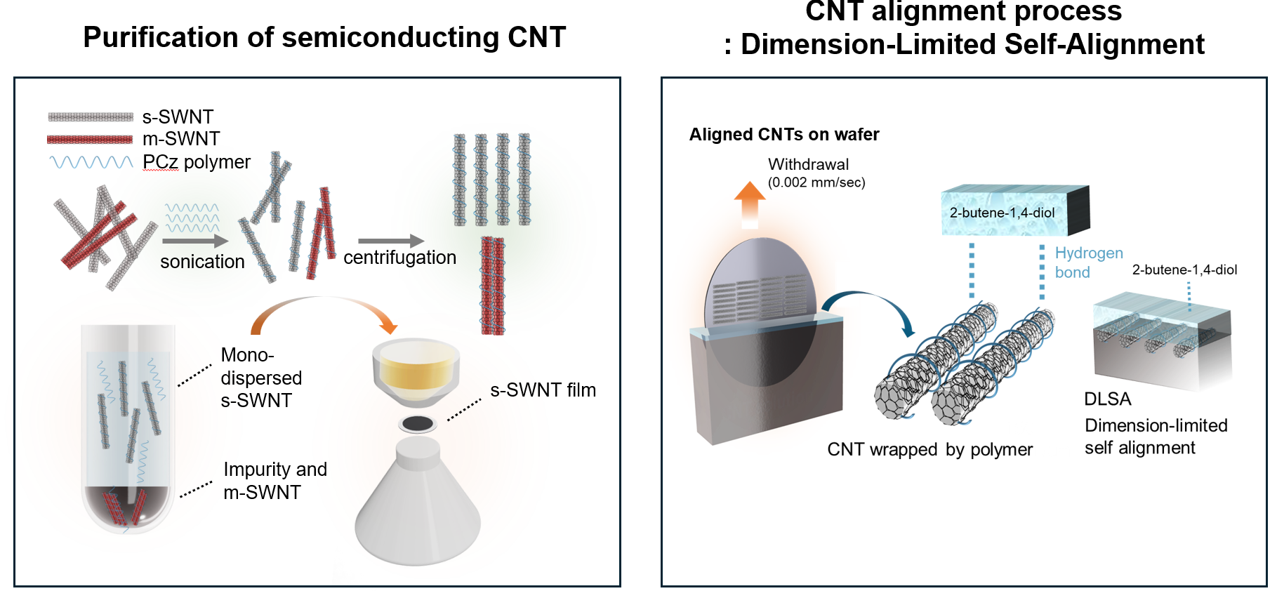
To utilize Carbon Nanotubes (CNTs) as a channel material, this research aims to purify high-purity semiconducting CNTs and fabricate high-density, uniformly aligned CNT films.First, 1) wrapping polymers will be employed in a solution-based process to separate metallic and semiconducting CNTs. By analyzing this mechanism, we aim to achieve a semiconducting CNT purity of over 99.9999%. To coat these purified CNTs onto a substrate in an aligned manner, 2) the Dimension-limited Self-Alignment (DLSA) method will be used. Through fluid dynamics and material analysis, we intend to enhance alignment precision and minimize CNT stacking. Furthermore, a novel alignment process will be developed to obtain highly ordered CNT films with consistent inter-tube spacing. Finally, by utilizing these aligned CNT films, we will 3) fabricate aligned CNFETs and implement them into next-generation device architectures, such as CFETs and GAA FETs.

High performance CNT-FETs

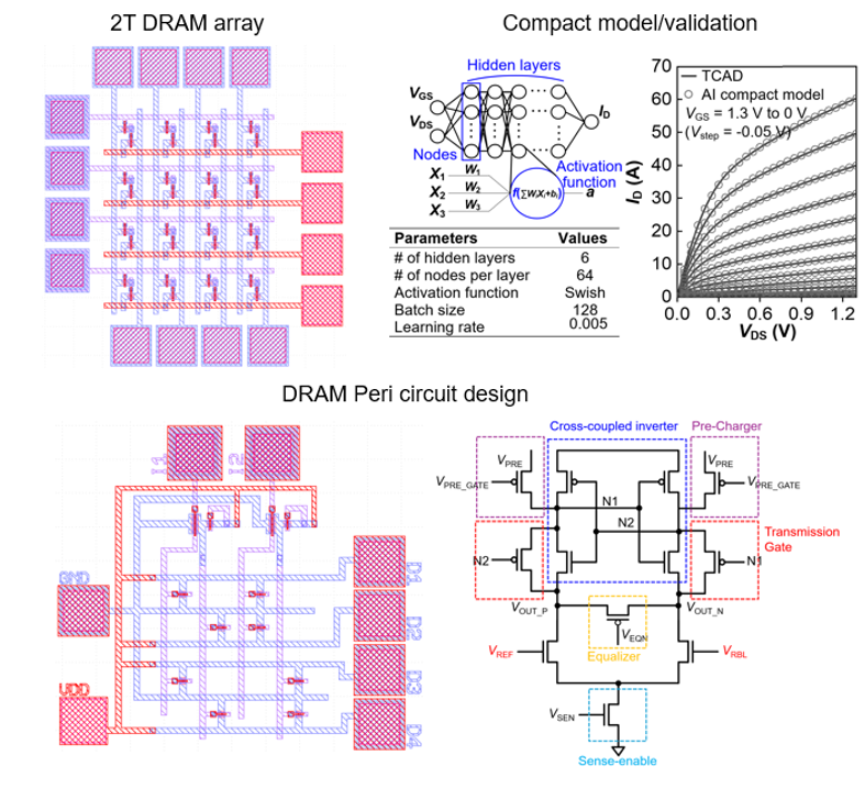
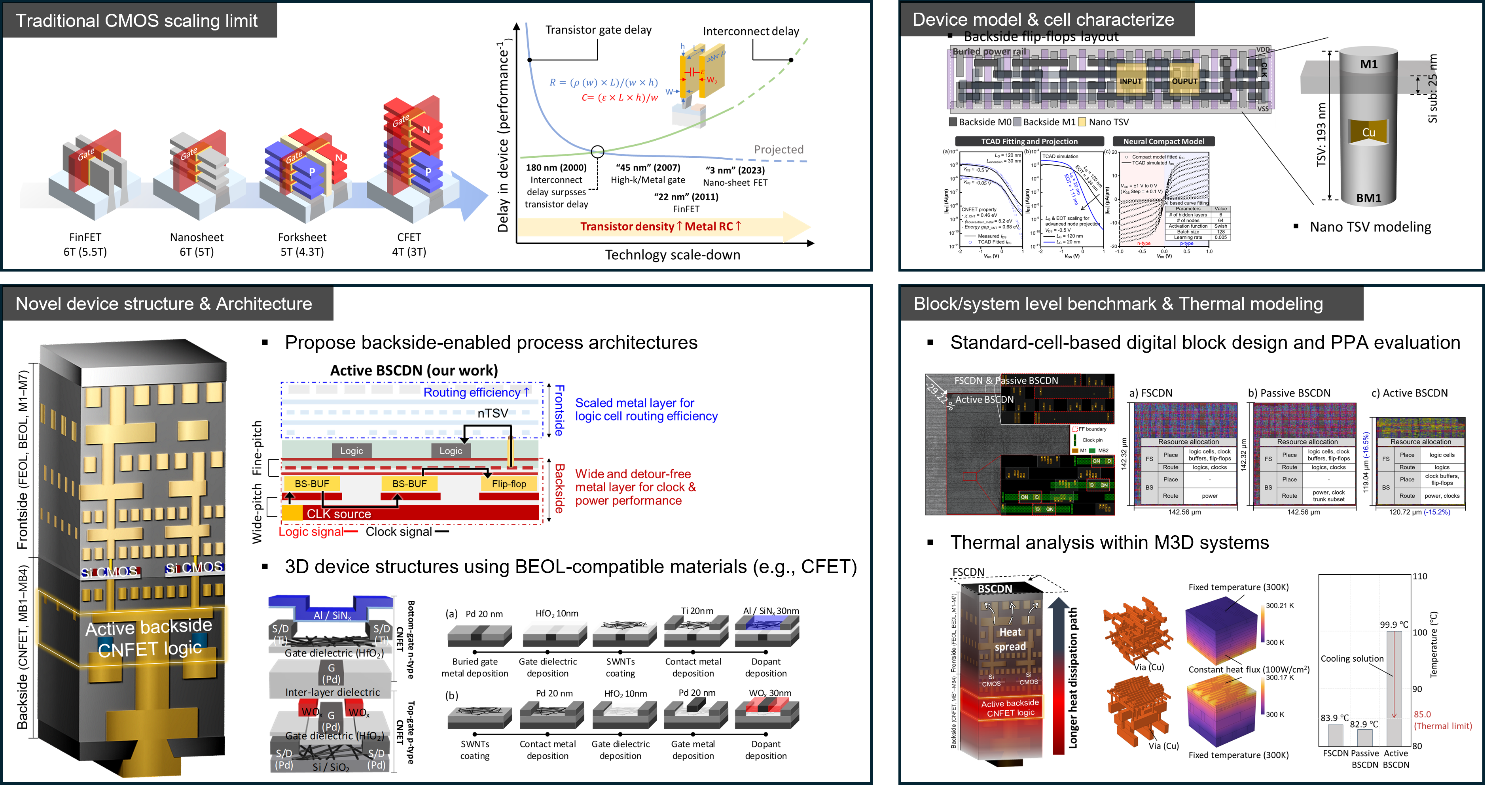
CNTs offer exceptional carrier mobility, high carrier density, and quasi-one-dimensional transport, enabling strong electrostatic control and high drive current. However, the small bandgap of CNTs leads to increased off-state leakage in MOSFET-like CNFETs, primarily due to band-to-band tunneling in gate-underlap and source/drain extension regions. Our research focuses on a structural solution that enables effective bottom-side doping of CNT channels while maintaining full compatibility with GAA architecture and BEOL-compatible integration schemes. Building on this device concept, we further explore vertically stacked CNFET-based CFET architectures and DTCO-driven standard cell optimization. Through block- and chip-level PPA benchmarking, our goal is to identify and extend the performance limits of low-dimensional-material-based logic technologies for future monolithic 3D systems.

Memory

Development of Oxide Semiconductor–Based Vertical Channel Transistor Device

We test and develop optimal process integration strategies to enhance the performance of oxide-based vertical channel transistors (VCTs). Recently, A novel fabrication strategy was employed to overcome the issues arising in VCT processing. (link) In particular, we employ TCAD-based device modeling to parameterize the impact of process variables on device characteristics and to conduct quantitative evaluations. Using TCAD structure editor (SDE) models, we systematically explore and validate process conditions and propose advanced and novel device structures. Furthermore, TCAD simulations enable analysis of position-dependent distributions of electrostatic potential, electric field, and current density, which are difficult to directly observe through experimental measurements.

High performance ALD Film Development

In the three-dimensional architecture of vertical channel transistors, atomic layer deposition (ALD) is essential to achieve uniform and conformal deposition of the channel layer. We investigate the composition ratios of constituent elements, film thickness, and doping strategies to deposit high-quality oxide ALD thin films. These films are evaluated not only through device-level performance metrics such as subthreshold swing (SS), drain current (ID), contact resistance (RC), and off-state current (IOFF), but also through a range of material characterization techniques, including X-ray photoelectron spectroscopy (XPS), X-ray diffraction (XRD), ultraviolet photoelectron spectroscopy (UPS), time-of-flight secondary ion mass spectrometry (ToF-SIMS), UV–visible spectroscopy, Raman spectroscopy, and Hall measurements.

Reliability Analysis from Device-level to Memory-level

Using high-performance ALD thin films optimized through VCT process and structural engineering, we evaluate the reliability of individual devices through standard stress tests, including time-dependent dielectric breakdown (TDDB), positive/negative bias stress (PBS/NBS), and positive/negative bias temperature instability (PBTI/NBTI). In addition, memory-level reliability metrics—such as retention, operation speed, and endurance—are systematically assessed. Ultimately, we investigate device- and array-level operation scenarios to analyze performance variations induced by charge loss and threshold voltage (Vth) shifts, and their impact on operation speed, retention time, and sensing errors in memory array operation.

Memory array / Peripheral Circuit Design for AI Computing

Peripheral circuits optimized for high-density DRAM arrays based on oxide-semiconductor vertical channel transistors (VCTs) are designed, and TCAD mixed-mode simulations are used to quantitatively analyze read/write, sensing, and retention behaviors under realistic operating conditions that include the coupled effects of the cell, peripheral circuits, and interconnect parasitics. In addition, compact models of oxide-semiconductor transistors are developed and integrated into SPICE-based array-level simulations. Based on this physics-aware modeling framework, the DRAM cells are further extended into PIM (Processing-in-Memory) and CIM (Compute-in-Memory) architectures, enabling a systematic evaluation of oxide-semiconductor-based memory–compute integrated architectures for AI acceleration.

DTCO/STCO

Monolithic 3D Logic Integration and Block/System-Level PPA Evaluation

This project focuses on block- and system-level design and benchmarking studies for monolithic 3D integration (M3D) systems. Standard cells, which underpin modern digital circuits, have advanced by reducing the cell height to increase cell density. However, this trend has intensified routing congestion, and the reduction in metal pitch has increased BEOL parasitics, bringing conventional scaling methods close to their practical limits. To overcome these constraints and sustain scaling, the field is exploring new integration directions beyond simple area reduction—such as proposing three-dimensional cell structures (e.g., CFET, 3DS-FET) or adopting architectural innovations like backside power delivery. Based on device-, standard cell-, and system-level evaluation and analysis, our lab aims to propose new directions and an application roadmap for three-dimensional integration that can extend scaling beyond the limits of CMOS downscaling.

[1] Yehyun Shin et al., "Active BSCDN benchmark framework with backside-compatible CNFET logic technology," 2025 71th IEEE International Electron Devices Meeting (IEDM), 2025.

Advanced Packaging

Advanced Packaging Technologies for High-Speed Interconnections

This project aims to develop advanced packaging solutions that comprehensively integrate electrical, mechanical, and thermal characteristics to enable high-speed and high-reliability signal transmission in chiplet-based heterogeneous integration and next-generation semiconductor systems.

Current packaging technologies are confronting multifaceted challenges, such as high-density I/O interconnects for ultra-fast inter-chiplet data transfer, efficient thermal management, and the maintenance of signal integrity in multilayered architectures. To overcome these hurdles, our laboratory employs design methodologies rooted in electrical and thermal simulations, allowing for the proactive prediction and optimization of signal interference, impedance mismatch, and thermal hotspots.

Building on this foundation, we are systematically advancing core component technologies for seamless chiplet integration, including via filling, bump growth, single/multilayer RDL (Redistribution Layer) fabrication, and advanced chip bonding techniques.

3D Printed Substrate

Curved Through Hole Interposers for Advanced Packaging

Design scaling has shifted from large monolithic dies to chiplet-based 2.5D/3D heterogeneous integration as die size approaches the reticle limit, making interposers a key platform for high-bandwidth, low-latency die-to-die interconnects and power delivery. However, conventional RDL stack-up fan-out interposers suffer from rising manufacturing complexity and cost due to multilayer build-up, repetitive lithography/plating/etch, accumulated misalignment, and limited via/routing freedom. In this work, high-resolution 3D printing directly forms curved-hole structures in a fan-out interposer to enable a continuous 3D transition (instead of a purely vertical via), mitigating impedance discontinuities and parasitics while reducing process complexity by defining 3D holes and wiring in a single fabrication step. Reverse-pulsed plating provides uniform metallization along the curved path and suppresses defects (underfill, seams, porosity) that increase loss and reflection. Future work will validate S-parameters, impedance continuity, mode conversion, and near-field coupling via CST-based 3D EM simulations and optimize the insertion-loss/return-loss/crosstalk trade-off by analyzing parasitic L/C distribution and return-path-induced common-mode components. Ultimately, this approach offers a practical route to next-generation 3D fan-out interposer platforms with improved design freedom and electrical reliability under cost and complexity constraints.

Integrated RF Components Embedded 3D-Printed Lid Substrate

The surge in mobile data traffic driven by next-generation networks such as 5G is rapidly pushing wireless systems toward the millimeter-wave (mmWave) spectrum. While mmWave enables ultra-high data rates and low-latency links through wide available bandwidth, higher operating frequencies increase conductor and dielectric losses and amplify parasitic reactance and radiation leakage at discontinuities in transmission lines, vias, and pads, making RF front-ends highly sensitive to process variations and structural defects. Conventional multilayer LTCC-based Antenna-in-Package (AiP) relies on stacking and vertical via stacks, which increases process complexity and cost, while via-stack misalignment induces impedance discontinuities and radiation leakage that degrade mmWave operation. To address these limitations, this work proposes a high-resolution 3D-printed lid substrate with embedded quasi-coaxial through-holes, where a via-fence defines the return path and suppresses field leakage to mitigate radiation loss and EMI. By fabricating vias, cavities, and a patch antenna in a single step and optimizing the design for a 28-GHz resonance, the proposed platform reduces alignment-induced discontinuities and suppresses insertion loss, reflection, and radiation leakage.

RF Packaging

RF Packaging for Broadband and Advanced Computing Systems

Next-generation communication and high-performance computing systems require RF packaging technologies that simultaneously support broadband signal transmission and high integration density. However, conventional RF packaging approaches based on wire bonding and flip-chip bonding suffer from fundamental limitations in bandwidth and signal integrity due to bonding-induced parasitics and insertion loss. This research aims to overcome these limitations by developing bonding-free, chip-embedded RF packaging architectures and RF MMIC structures based on low-loss glass substrates. By embedding active RF chips directly within the substrate and integrating RF matching networks and passive components on glass, discontinuities and losses at the chip–substrate interface are significantly reduced. In addition, this work explores CNFET-based RF power amplifier (PA) designs compatible with BEOL processes, enabling tighter integration of RF circuits with digital ICs. Furthermore, electrical–thermal co-design using through-glass vias (TGVs) is investigated to efficiently dissipate heat generated during high-power RF operation, thereby ensuring stable and reliable high-frequency performance.

Quantum Packaging for Cryogenic Quantum Computing Systems

In quantum computing systems, packaging technologies play a critical role in reliably interfacing qubits operating at cryogenic temperatures with electronic systems for readout and control. These requirements are fundamentally different from those of conventional room-temperature RF packaging. This research focuses on interposer and RF circuit packaging technologies optimized for cryogenic environments, based on an in-depth understanding of quantum computing system architectures. RF circuits for qubit readout and control are designed alongside cryogenic low-noise amplifiers (LNAs) and RF components, enabling signal transmission structures tailored to quantum systems. In addition, cryogenic interposer and interconnection structures using superconducting materials are investigated to minimize signal loss at ultra-low temperatures and to provide scalable packaging architectures for large-scale qubit systems.