[Media Coverage] Turning a Memory Material into a Logic Device — Nature Communications Paper in the News
- Work by Prof. Jimin Kwon’s group at KAIST DSIL, in collaboration with Prof. Yong-Young Noh’s group at POSTECH, on wafer-scale non-ferroelectric κ-phase In₂Se₃ logic transistors has been published in Nature Communications and covered by major Korean media outlets.
Featured coverage:
-
[ETNews] POSTECH and KAIST demonstrate κ-phase indium selenide logic transistors at 4-inch wafer scale (link)
-
[KPI News] A semiconductor material that only “remembered” now extends to “thinking” (link)
-
[Gyeongbuk Shinmun] POSTECH–KAIST turn a “remembering” semiconductor material into a “judging” logic device (link)
Dongjin Wi Selected for the NRF Master's Research Fellowship (2026)
- Dongjin Wi was selected for the NRF Master’s Research Fellowship program.
The program supports full-time master’s students by providing one year of funding for thesis research and early-stage researcher development.
Dr. Youngmin Jo Selected for the NRF Basic Research Program B (Inclusive Type)
-
Dr. Youngmin Jo, a postdoctoral researcher, has been selected for the 2026 Basic Research Program B (Inclusive Type) under the Ministry of Education’s Academic Research Support Program in Science and Engineering, administered by the National Research Foundation of Korea (NRF).
-
Selected project: Oxide Heterojunction Tunnel Field-Effect Transistors for Ultra-Low-Power Embedded Memory Systems
The program broadens the research base in science and engineering by offering diverse research opportunities to non-tenure-track faculty and postdoctoral researchers at universities, providing 60 million KRW per year (including indirect costs) for three years (Sept. 1, 2026 – Aug. 31, 2029).

Dr. Yongwoo Lee Receives Best Poster Award at IMID 2026
-
Title: Electrochemically programmable organic mixed ionic-electronic conductors for GHz impedance tunable radio-frequency electronics
Dr. Yongwoo Lee received the Best Poster Award at the International Meeting on Information Display (IMID), held at BEXCO in Busan.
[Media Coverage] KAIST Solves 3D Memory Challenges to Boost AI Semiconductor Efficiency
- Our research on 3D oxide vertical channel transistors (VCTs) and ‘Oxygen Tunnel’ technology for AI semiconductors has been featured in domestic media outlets.
Featured Articles:
-
[Herald Corp] KAIST Solves 3D Memory Challenge to Boost AI Semiconductor Performance and Energy Efficiency (link)
-
[TechWorld] KAIST Enhances Power Efficiency of AI Semiconductors: Resolving 3D Memory Challenges with ‘Oxygen Tunnels’ (link)
-
[News1] KAIST Opens New Era for 3D AI Memory via Dedicated ‘Oxygen Passageways’ (link)
![[Front Cover] Oxygen-Tunnel ITO Vertical-Channel Transistors Featured in Advanced Functional Materials](/assets/img/news/2026-03-%EA%B5%AC%ED%98%84%ED%98%B8-AFM-%EC%A0%84%EB%A9%B4%ED%91%9C%EC%A7%80%EC%84%A0%EC%A0%95.jpg)
[Front Cover] Oxygen-Tunnel ITO Vertical-Channel Transistors Featured in Advanced Functional Materials
-
Our research on oxygen-tunnel ITO vertical-channel transistors has been featured on the Front Cover of Advanced Functional Materials (Volume 36, Issue 66, August 17, 2026).
-
This study (first author: Hyeonho Gu) proposed an oxygen-tunnel (SiN/SiO₂/SiN) architecture for indium tin oxide (ITO) vertical-channel transistors. The proposed structure precisely controls oxygen transport, achieving a record-high current density and enabling simultaneous improvement of drive current and reliability for monolithic 3D embedded memory.
-
The Front Cover of Advanced Functional Materials is carefully selected by the editorial board to highlight research that demonstrates exceptional scientific quality and broad significance within the issue.
-
Paper Link: link
-
Cover Link: link
Dr. Yongwoo Lee Selected for the NRF Postdoctoral Researcher Growth Support Program
- Dr. Yongwoo Lee has been selected for the Independent Research Track of the Postdoctoral Researcher Growth Support Program, funded by the Ministry of Education and the National Research Foundation of Korea (NRF).
-Project Title: Development of Core Technologies for Highly Reliable Glass Substrate-Based Packaging with Embedded mmWave GaN RF PAs for Physical AI Humanoids. (link)
This program supports promising postdoctoral researchers in conducting innovative and challenging research under the mentorship of a faculty member, enabling them to grow into independent researchers. The selected researcher will receive KRW 60 million annually for three years.
[Media Coverage] KAIST Develops Automated Sorting Technology for 2D Semiconductors
- Our research on automated sorting and transistor fabrication for 2D semiconductors has been widely featured in domestic media outlets.
Featured Articles:
-
[DigitalToday] KAIST Develops Automated Sorting Technology for 2D Semiconductors (link)
-
[Asia Business Daily] Automating the Sorting and Transistor Fabrication of “Dream” 2D Semiconductors (link)
-
[Donga Science] Automating 2D Semiconductor Flake Sorting and Device Fabrication (link)
Led by Prof. Jimin Kwon’s team, this study introduced an automated platform that classifies 2D semiconductor flakes by thickness via optical microscopy and automatically fabricates transistors. By analyzing over 120,000 flakes and 1,615 devices, the research established a data-driven foundation for thickness-dependent charge transport analysis, with the findings published in Advanced Functional Materials.
Dr. Haksoon Jung Published in Advanced Materials 2026
Title: Monolithic 3D-Integrated All-Solid Ion-Gated Carbon Nanotube Transistors With Tunable Ionic Conductance for Multi-Timescale Reservoir Computing (link)
In this study, we propose all-solid ion-gated transistors (sIGTs) with semiconducting carbon nanotube (CNT) channels that enable wide-range engineering of ionic dynamics while remaining fully compatible with scalable thin-film processing.
By precisely tuning the ionic content and thickness of the solid ionogel down to the sub-micron regime, ionic time constants ranging from microseconds to milliseconds were achieved within an identical device geometry.
Electrical impedance spectroscopy (EIS) and small-signal analysis were used to systematically reveal the relationship between ionic conductance and frequency-dependent device response, and uniform, reliable device characteristics were demonstrated at up to 4-inch wafer scale as well as on flexible substrates.
At the system level, two CNT sIGT layers with distinct ionic dynamics were vertically integrated through monolithic 3D (M3D) stacking to realize a dual-timescale physical reservoir capable of classifying time-varying input signals using a single readout layer.
This work demonstrates the potential of sIGTs as a scalable hardware platform for multi-timescale signal processing in neuromorphic computing.
This research was supported by the National Research Foundation of Korea (NRF), the Korea Planning & Evaluation Institute of Industrial Technology (KEIT), the Ministry of Science and ICT (MSIT), and the Ministry of Trade, Industry and Energy (MOTIE).
Hyeonho Gu Published in Advanced Functional Materials
- Title: Oxygen-Tunnel Indium Tin Oxide Vertical Channel Transistors with Enhanced Current Density and Reliability for Monolithic 3D Compute-In-Memory Systems (link)
This work proposes an oxygen-tunnel (SiN/SiO2/SiN) architecture for indium tin oxide (ITO) vertical-channel transistors, enabling simultaneous improvement of drive current and reliability for monolithic 3D embedded memory.
The proposed structure precisely controls oxygen transport, suppressing electrode oxidation while stabilizing the ITO channel, achieving a record-high current density of 436 μA/μm and excellent bias-stress stability.
Based on these devices, we demonstrated capacitor-less gain-cell memory with over 648 s retention and more than 1,200 write/read cycles.
System-level evaluations further showed that hybrid Si-CMOS/ITO integration can reduce memory cell area while extending data retention and improving compute-in-memory performance for next-generation AI hardware.
This research was supported by NRF, KEIT, and related Ministry of Science and ICT / MOTIE funding programs.
- Featured Article: [Herald Corp] KAIST Solves 3D Memory Challenge to Boost AI Semiconductor Performance and Energy Efficiency (link)
Dr. Yongwoo Lee's Paper Published in Nature Communications
- Title: Wafer-scale uniform non-ferroelectric κ-phase In₂Se₃ transistors (link)
This work proposes the underexplored non-ferroelectric κ phase of indium selenide (In₂Se₃), presenting a BEOL-compatible process that forms uniform films across a full 4-inch wafer using thermal evaporation and a 250°C anneal.
A 24×24 array of 576 devices achieved an average mobility of 39.3 cm²V⁻¹s⁻¹ and an on/off current ratio spanning more than eight orders of magnitude, and monolithic integration with a p-type Se-alloyed TeOₓ device yielded a full-swing complementary inverter.
The work was carried out by Prof. Jimin Kwon’s group at KAIST DSIL in collaboration with Prof. Yong-Young Noh’s group in the Department of Chemical Engineering at POSTECH and Prof. Ao Liu’s group at UESTC, with Dr. Yongwoo Lee of our group serving as co-first author alongside Jaeyun Lee of POSTECH.
Paper Co-First-Authored by Heesoo Yang and Hyeongjun Kim (Integrated M.S./Ph.D., 2nd year) Accepted to IEEE VLSI Symposium 2026
- Title : Vertical-Die (V-die) 3.5D Integration for Cool Ultrahigh-Bandwidth Memory Systems (link)
A paper by Heesoo Yang and Hyeongjun Kim (both 2nd-year integrated MS/PhD students) has been accepted at the IEEE Symposium on VLSI Technology and Circuits (VLSI) 2026, one of the most prestigious international conferences on integrated device and circuit technology. The work was carried out in collaboration with Hanbat National University (Prof. Seongju Kim) and UNIST (Prof. Dongyun Kam).
This work proposes a 3.5D V-die memory architecture in which DRAM dies are oriented upright on an interposer, addressing both the TSV-limited I/O scalability and the thermal constraints of conventional HBM.
Related coverage: [ETNews] Standing HBM upright quadruples bandwidth — accelerating “vertical die” development (link)
International coverage: [IEEE Spectrum] Stacking Chips Sideways Gives AI More Memory (link)
Sanghyeon Lee Published in Advanced Functional Materials
- Title: Statistically Resolving Thickness-Dependent Electrical Characteristics in Multilayer-MoS2 Transistors (link)
The study combines optical-intensity-based layer identification and algorithmic flake filtering to enable large-scale statistical analysis of multilayer MoS2 transistor behavior.
- Featured Article: [Asia Business Daily] Automating the Sorting and Transistor Fabrication of “Dream” 2D Semiconductors (link)
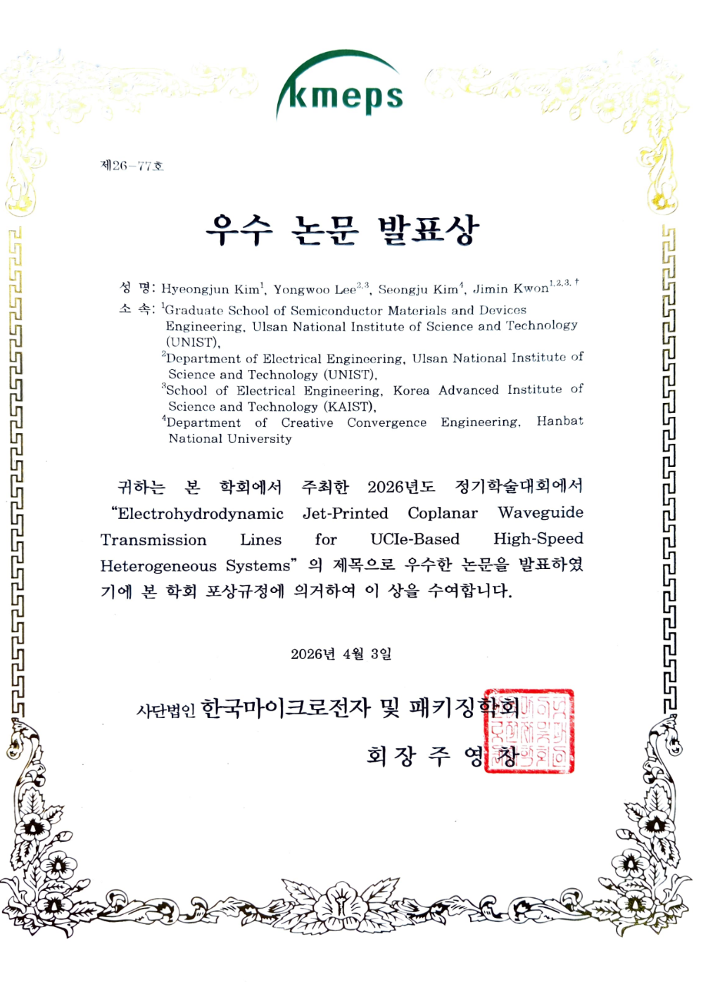
Hyeongjun Kim Received a Best Presentation Award at KMEPS 2026
- Title: Electrohydrodynamic Jet-Printed Coplanar Waveguide Transmission Lines for UCIe-Based High-Speed Heterogeneous Systems
Hyeongjun Kim received a Best Presentation Award at KMEPS 2026 for research on EHD jet-printed CPW transmission lines targeting UCIe-based high-speed heterogeneous systems.
Guhyun Ho Received the Graduate School Outstanding Thesis Award
Guhyun Ho received the Graduate School Outstanding Thesis Award for research on oxide-semiconductor vertical-channel-transistor-based 2T0C gain-cell memory.
Dr. Haksoon Jung Published in ACS Nano
- Title: Advances and future challenges in monolithic 3D integrated logic, power, and optoelectronics technologies for tightly interconnected intelligent systems (link)
The article presents a broad perspective on monolithic 3D integration and optoelectronic co-integration for next-generation AI and HPC systems, from materials to system-level design.
Guhyun Ho Published in IEEE Electron Device Letters
- Title: Indium Tin Oxide Vertical Channel Transistors for Scaled 4F2 2T0C Gain Cell Memory with Etched Sidewall Cleaning (link)
Oxide-based vertical-channel transistors can enable 4F2-class DRAM cells, but hole-etch residues contaminate sidewalls and limit scaling. This work identifies the degradation mechanism and demonstrates strong recovery through post-etch wet cleaning.
Hyeongjun Kim Won Best Poster Award at ISMP 2025
- Title: Development of Silver EHD Jet Printing Design Rules for Reliable RF Component Fabrication
Hyeongjun Kim received a Best Poster Award at the International Symposium on Microelectronics and Packaging (ISMP) 2025.
Selected for the Samsung Future Technology Program
- Project: V-die integrated packaging technologies for ultra-high-bandwidth AI accelerators
- Organization/Program Office: Samsung Electronics / Samsung Future Technology Incubation Center
- Participation/Period: Single-institution project / 2025.12.01 - 2030.12.31
Our lab was selected for the Samsung Future Technology Program to develop vertically integrated V-die packaging technologies for scalable AI accelerator systems.
Dr. Yongwoo Lee Published in Science Advances
- Title: Addressing Gain-Bandwidth Trade-off by Electrolyte-All-Around Organic Electrochemical Transistors (link)
The study introduces an electrolyte-surround architecture to improve ion transport dynamics and overcome the gain-bandwidth trade-off in OECTs.
Three Papers Accepted to IEEE IEDM 2025
- Thermal Evaluation and Comparison of CAA and GAA Indium Tin Oxide Vertical Channel Transistors
- Monolithic 3D Integration of III-V HEMTs on Glass Using Ultra-Thin Dielectric Bonding Layer
- Active BSCDN Benchmark Framework with Backside-Compatible CNFET Logic Technology
Three papers submitted by our students were accepted simultaneously to IEEE IEDM 2025. The work was conducted in collaboration with Stanford University (Prof. Eric Pop, Prof. H.-S. Philip Wong), KAIST (Prof. Sanghyeon Kim), and UNIST (Prof. Heechun Park).
Three Students Selected for the NRF Master's Research Fellowship (2025)
Seunghun Baek, Hyeongjun Kim, and Heesoo Yang were selected for the NRF Master’s Research Fellowship program.
The program supports full-time master’s students by providing one year of funding for thesis research and early-stage researcher development.
Dr. Seongju Kim Appointed Assistant Professor at Hanbat National University
Dr. Seongju Kim was appointed as an Assistant Professor in the Department of Convergence and Creativity at Hanbat National University.
Selected for the Quantum Core Technology Development Program
- Project: Development of microwave signal generation and processing hardware for quantum system control
- Ministry/Agency: Ministry of Science and ICT / National Research Foundation of Korea (NRF)
- Participation/Period: Consortium project / 2025.07.01 - 2027.12.31
Our lab was selected for the Quantum Core Technology Development Program to develop an FPGA-based RF front-end platform with integrated LO, filtering, amplification, and control modules.
Dr. Haksoon Jung Selected for NRF Postdoctoral Growth Program
- Project: Development of AI- and 3D-printing-based high-thermal-performance semiconductor packaging technologies
- Program: NRF Postdoctoral Growth Support Program (Ministry of Education / NRF)
Dr. Haksoon Jung was selected for the NRF Postdoctoral Growth Support Program, which supports postdoctoral researchers with multi-year funding and mentoring toward independent research careers.
Dr. Seongju Kim and Dr. Haksoon Jung Received Top Awards at KIEEM 2025
- Dr. Seongju Kim: Reinforcement-learning-based optimal cooling-channel design for advanced semiconductor packaging
- Dr. Haksoon Jung: 3D-printed organic fan-out substrates for advanced semiconductor packaging
Both researchers received top awards at the 2025 KIEEM Summer Conference.
Minho Park Won a Best Paper Award at KCS 2025
- Title: Top-Gate Oxide Semiconductor FETs for Reliable 2T0C Read/Write Operation with Reduced Capacitive Coupling (link)
Minho Park received a Best Paper Award at KCS 2025.
Nahyeon Kim and Hyeongjun Kim Won Best Presentation Awards at KFPE 2025
- Nahyeon Kim: 3D-Printed Quasi-Coaxial Through-Hole Embedded Substrate for Antenna-in-Package Applications
- Hyeongjun Kim: Fabrication of RF Transmission Lines and Antenna Using Electrohydrodynamic Inkjet Printing
Two students from our lab received Best Presentation Awards at KFPE 2025.
Nahyeon Kim Won an On-site Best Poster Award at KCS 2025
- Title: 3D-Printed Antenna-in-Package Substrates with Quasi-Coaxial Through-Vias for 5G-Advanced Applications
Nahyeon Kim received an On-site Best Poster Award at the Korean Conference on Semiconductors (KCS) 2025.
Dr. Haksoon Jung Published in ACS Nano
- Title: Back-end-of-line-compatible passivation of sulfur vacancies in MoS2 transistors using electron-withdrawing benzenethiol (link)
This work introduces a BEOL-compatible sulfur-vacancy passivation strategy for MoS2 transistors and demonstrates strong performance and reliability improvements through process-compatible defect engineering.
Sumin Hong Won a Best Presentation Award at KFPE 2024
- Title: Fabrication of top-gate MoS2 FETs via gate-dielectric seed-layer optimization
Sumin Hong received a Best Presentation Award in the graduate student oral session at the KFPE 2024 Fall Conference.
Prof. Jimin Kwon Received the KFPE Young Scholar Award
Prof. Jimin Kwon received the 2024 Young Scholar Award from the Korean Society of Flexible and Printed Electronics (KFPE) in recognition of outstanding contributions as an emerging researcher.
Dr. Yongwoo Lee Selected for the NRF Domestic Postdoctoral Fellowship
- Project: Printed organic electrochemical transistor technologies for next-generation communication systems
- Program: NRF Domestic Postdoctoral Fellowship
Dr. Yongwoo Lee was selected for the NRF Domestic Postdoctoral Fellowship program, which provides opportunities for Ph.D. researchers to continue advanced research at leading institutions in Korea.
Three Students Selected for the NRF Master's Research Fellowship
Students Guhyun Ho, Hyeonjin Lee, and Nahyeon Kim were selected for the NRF Master’s Research Fellowship program.
The program provides full-time master’s students with one year of support to conduct thesis research and strengthen early-stage research capability.
Dr. Yongwoo Lee and Haksoon Jung Published in IEEE Electron Device Letters
- Title: Dual-gate carbon nanotube thin-film transistors with printed channel and passivation interlayer on plastic foil (link)
This work reports high-performance printed CNT transistors using a dual-gate architecture and polymer interlayer engineering to improve gate controllability and suppress leakage. The study demonstrates a scalable route toward reliable printed electronics for advanced circuits.
Dr. Yongwoo Lee Published in npj Flexible Electronics
- Title: Stabilizing Schottky junction in conjugated polymer diodes enables long-term reliable radio-frequency energy harvesting on plastic (link)
Long-term diode stability is critical for wireless power transfer in wearable systems. We identified unstable chemical bonding at the semiconductor-cathode interface as the key degradation mechanism in flexible organic diodes. Through comprehensive analysis and interlayer engineering, we demonstrated a Schottky diode with stable operation over several months. This work was supported by NRF and IITP.
Related coverage: ETNews, Yonhap News
Nahyeon Kim Presented at ECTC 2024
- Title: Micro-3D-printed packaging substrates with embedded through holes for organic interposers (link)
Semiconductor system performance is increasingly determined by how chips are interconnected through packaging technology. In this work, we proposed a new process to fabricate packaging substrates with through-holes using micro 3D printing. Fine through-holes were formed without etching, reducing process complexity while increasing design flexibility. We also developed a reliable inner-hole metallization process, demonstrating broad applicability to advanced packaging substrates. This work was supported by NRF and IITP.
Selected for the National Semiconductor Laboratory Core Technology Program
- Project: Core technology development for 3D-printing-based semiconductor packaging
Our lab was selected for the National Semiconductor Laboratory core technology support program in advanced semiconductor packaging. A total of 9 labs (first half) and 10 labs (second half) were selected nationwide, and this was the first selection from UNIST. The project is supported by the 3D Printing Center and Ulsan Metropolitan City.
Related coverage: Seoul Economic Daily, UNIST News Center